Introduction
Two-dimensional (2D) materials are a class of atomically-thin materials with unique electronic properties that can be exploited to build novel quantum electronics. Initially, carbon was assumed to be the only element with a stable isolatable 2D material phase (graphene) until a new class of compounds called transition metal dichalcogenides (TMDs) were found to also have the same property. While graphene is a conductor with a zero bandgap, TMDs are semiconductors with finite bandgaps, which can be exploited for semiconductor electronics. Moreover, the bandgap of these TMDs is also a function of their layer number, allowing for bandgap engineering. Due to their atomic thickness, TMDs can be theoretically used to create smaller and more efficient transistors. However, despite their potential for future technology, the synthesis of these quantum materials has been a difficult task due to engineering challenges.
Objective
The goal of this experiment is to use machine learning (ML) to optimize the chemical vapor deposition (CVD) process used to synthesize high-quality atomically-thin optoelectronic-grade molybdenum disulfide (MoS2), a member of the TMD family. Furthermore, after growing the monolayer MoS2 crystals, characterization is to be done using Raman and PL spectrometry along with atomic force microscopy.
Method
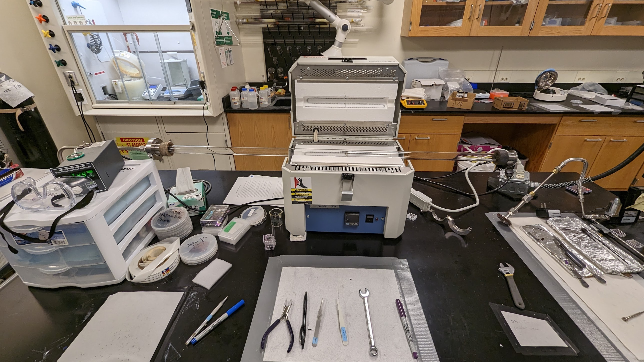
The experiment starts by setting up the Chemical Vapor Deposition (CVD) system (shown in Fig. 1), consisting of an induction furnace, a quartz tube, a gas flow system, a substrate (either a silicon or quartz wafer), two combustion boats for reactants (MoO2 and sulfur powder), and necessary connections for gas flow and vacuum creation.
For the CVD process, five crucial Design of Experiment (DoE) parameters are considered: the ramping rate, holding time, positions of the sulfur and sample boats, and the flow rate of argon gas. These DoE parameters constitute the 5D design space. The optimization problem involves finding a coordinate in the design space which would produce high-quality monolayer optoelectronic MoS2.
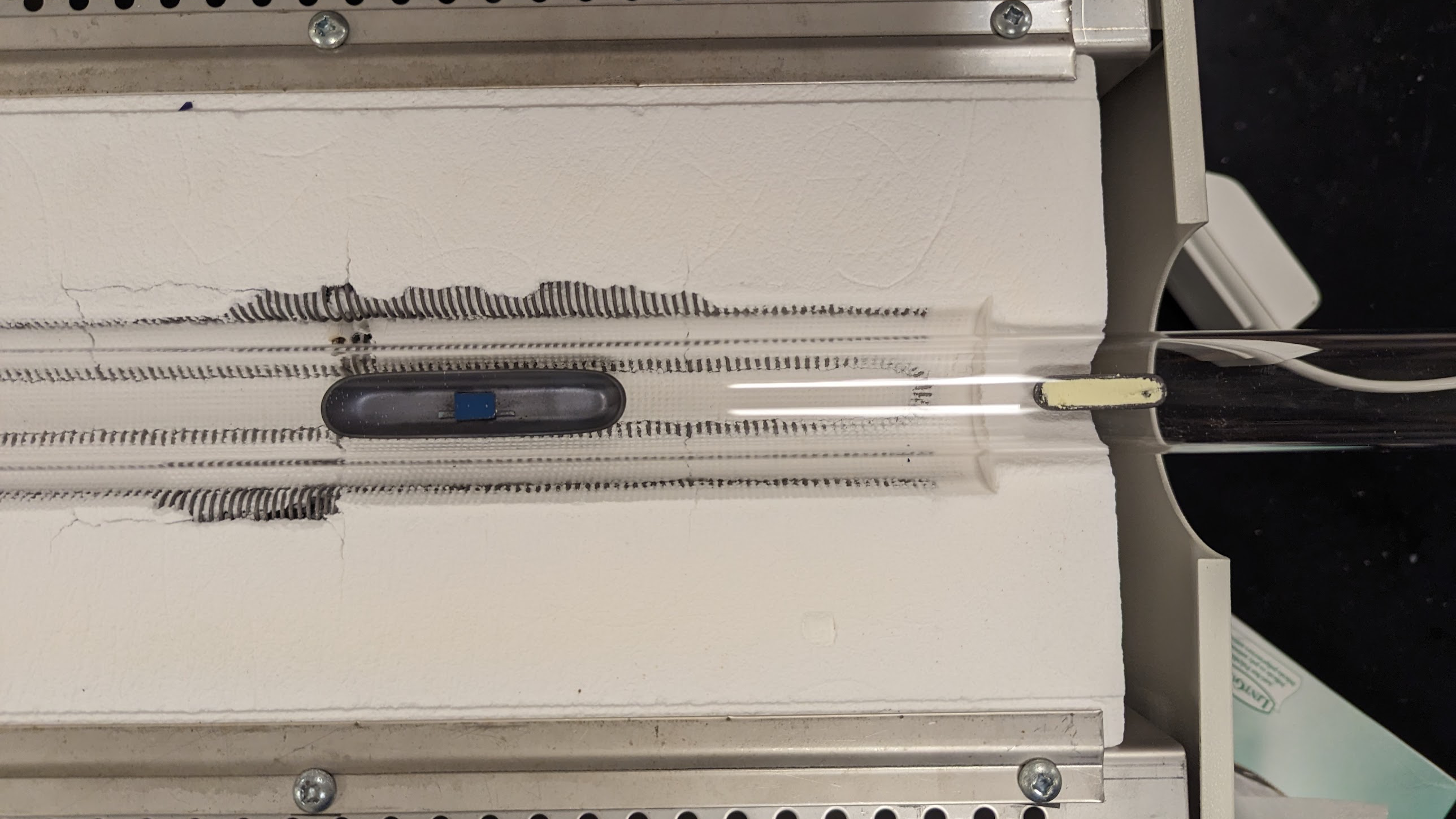
Initially, crystal growth parameters are assumed for the CVD process based on prior calculations and literature review. The quartz tube is cleaned and then placed in the furnace such that the furnace heats its middle portion. The quartz tube is connected on one side to the pressurized argon gas cylinder via a swagelok tube and a digital flow rate sensor. On the other side, the quartz tube is connected to a roughing pump that creates a vacuum inside the tube and the pressure in the tube is displayed using a digital barometer. For the CVD process, two combustion boats are used to hold the reactants. The sulfur boat is filled with the sulfur powder to the brim and a pinch of MoO2 powder is sprinkled in the sample boat. The silicon/quartz wafer piece is placed above the MoO2 powder using tiny rectangular silicon wafer pieces acting as ledges, such that the powder does not touch the wafer piece. The swagelok connecting the tube to the argon gas is opened and the boats are carefully placed at their designated locations inside the tube with the help of a hooked metal rod (shown in Fig. 2).
The swagelok is again secured and the process is ready to begin. A vacuum is first produced in the tube to remove all airborne impurities and then the argon gas is allowed to flow through the tube at a constant flow rate. Then a predefined temperature profile is used for the CVD reaction. The temperature ramp rate of the furnace reactor is manually adjusted as per the profile. The furnace is initially quickly brought to a temperature of 520 °C and then slowly brought to a temperature of 712 °C based on a specific ramp rate. Then, after the furnace reaches 712 °C, the temperature is held for a specific amount of time. Thus, the CVD process is meticulously controlled, adjusting parameters like temperature, gas flow rates, and timing to encourage the growth of monolayer MoS2 on the wafer pieces.
Post-growth, the MoS2 layers are characterized using Raman spectroscopy, atomic force microscopy (AFM), and photoluminescence (PL) spectroscopy to assess their quality and structural properties. Raman spectroscopy evaluates layer thickness and uniformity, AFM provides morphological data, and PL spectroscopy investigates the optical properties, including the bandgap and electronic structure. The optoelectronic quality is determined by analyzing the A-exciton linewidth (σA) in the PL spectrum.
Machine learning techniques, specifically classification and regression models along with a Bayesian Optimization (BO) query generator, are employed to optimize the growth process. These methods help in identifying promising areas of the experimental design space and in predicting how adjustments in conditions impact material quality. By intelligently navigating the design space, these machine learning components streamline the synthesis process, accelerating the discovery and optimization of new materials in a data-driven manner.
Results
The ML-guided approach demonstrates a systematic improvement in the quality of MoS2 crystals over several iterations. This includes moving from unsatisfactory growth to abundant growth of monolayer flakes with narrow σA values, indicative of high optoelectronic quality (shown in Fig. 3). The approach significantly reduces the number of experiments needed to optimize the CVD process, demonstrating about an 85% reduction in experimental trials compared to a traditional unguided approach.

Discussion
The iterative experiments provide detailed insights into the CVD furnace’s performance, allowing for precise adjustment of parameters to achieve the desired quality of 2D MoS2 crystals. The project validates the performance of the ML models through additional experiments, confirming their ability to accurately predict the optimal conditions for CVD synthesis and to distinguish between successful and unsuccessful experimental setups.
Beyond the quality of the MoS2 crystals, the ML-guided approach also leads to improvements in the morphology of the grown crystals, with larger flake sizes and higher surface coverage of monolayer crystals being achieved in later iterations.
Conclusion
In summary, the research study not only demonstrates a significant advancement in the synthesis of high-quality MoS2 but also sets a precedent for the application of ML in material science. The approach reduces the barrier to entry for material discovery and optimization, offering a scalable, efficient pathway towards the development of next-generation materials. This progression towards integrating ML into material synthesis heralds a new era of research and development, characterized by faster discoveries, reduced costs, and the realization of materials with unprecedented properties.
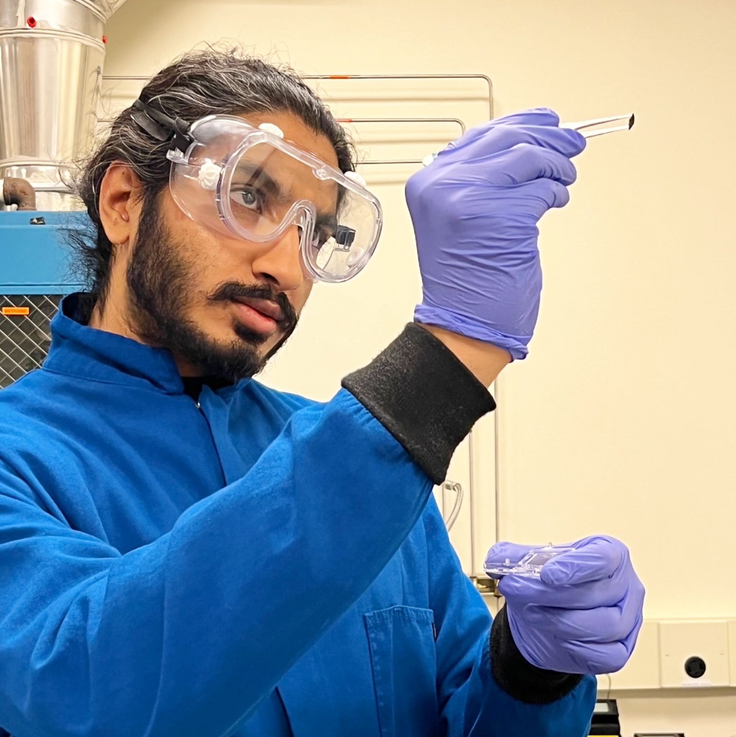
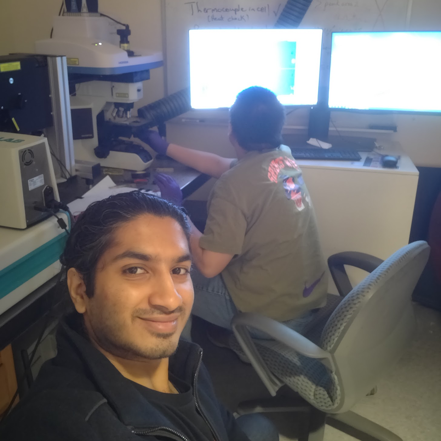
Photo Gallery