Introduction
Micro-Electro-Mechanical Systems (MEMS) pressure sensors have increasingly become critical components in various applications, especially in environments characterized by extreme conditions such as high temperatures, strong radiation, corrosive media, and high pressures. These harsh environments are commonly found in industries such as aerospace, automotive, oil and gas, and nuclear power generation. The unique challenge presented by such conditions is the need for sensors that not only accurately measure pressure but also withstand and operate reliably within these extreme settings. MEMS pressure sensors, thanks to their small size, high sensitivity, and potential for integration with electronic circuits, offer several advantages over traditional pressure sensing technologies. For applications in harsh environments, MEMS sensors are often designed with specialized materials and fabrication processes to enhance their durability and operational lifespan. The development and integration of these sensors contribute significantly to enhancing safety, reliability, and efficiency in sectors where failure can have severe consequences.
Objective
The goal of this research project is to design and fabricate high-quality scandium-doped aluminum nitride-based piezoelectric surface acoustic wave (SAW) MEMS pressure sensors for applications in nuclear electro-refineries.
Method
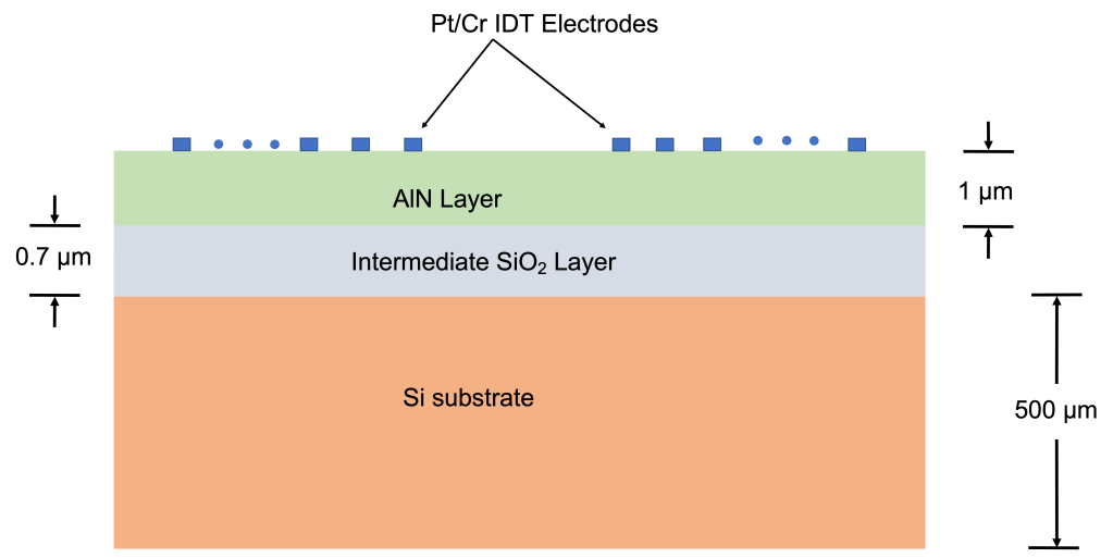
The research project work started initially by performing a thorough literature review. The operating principles of SAW devices was deeply studied and then crucial design parameters for SAW pressure sensors such as pressure sensitivity, temperature coefficient of frequency (TCF), dynamic ranges of pressure and temperature, resonant frequency, and Q-factor were identified. A substrate material stack made of ScAlN (1 μm)/SiO2 (0.7 μm)/Si (500 μm) with a thickness and an electrode material stack of Pt (10 nm)/Cr (200 nm) were chosen for the SAW devices (shown in Fig. 1).
Based on the literature review, sensor dimensions were chosen to be Furthermore, the equivalent electrical circuit models for SAW resonators were studied. Next, via the COMSOL simulations, two SAW center frequencies were chosen. Based on this, the design parameters were electrode width and number of IDT fingers. The electrode widths were 1.75 μm and 3.75 μm, and number of IDT fingers were 30, 40, and 50. Thus, there were 6 combinations of devices to try, all of which were designed to be produced on one die. A total of 57 dice were also planned to be fabricated, giving a total of 342 devices.
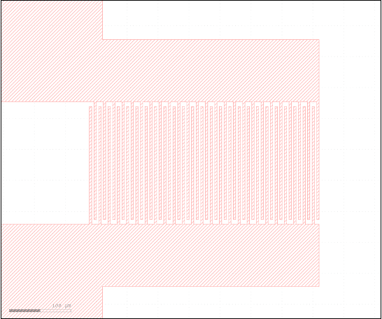
Thus, a layout for the 342 devices was planned using the PHIDL package in python via Jupyter notebook and converted to a GDS file using the software Klayout. The GDS file was sent to a mask manufacturer and a photolithography chrome mask was obtained.
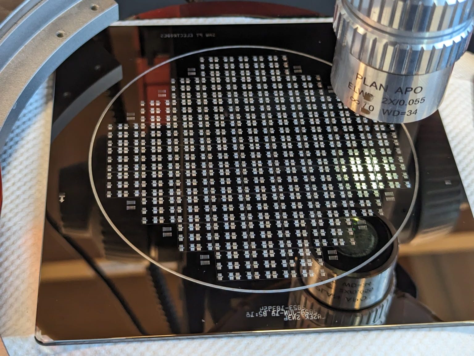
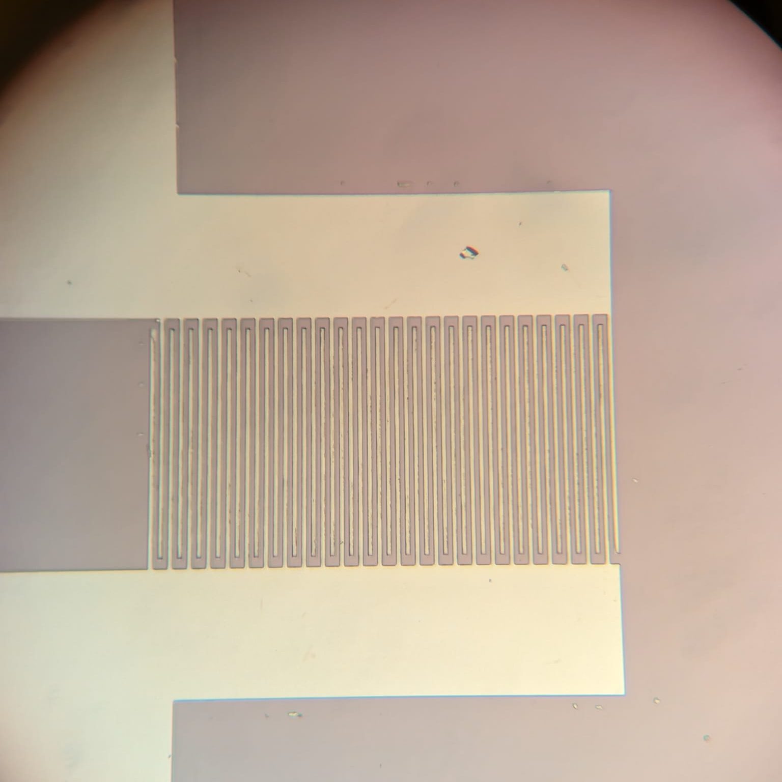
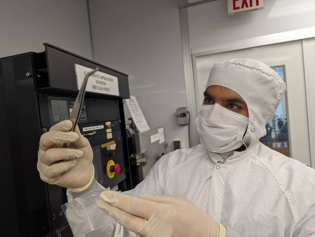
Using this mask, photolithography on a test silicon wafer (after spin-coating it with photoresist S1813) was done iteratively to figure out the right recipe. Finally, the ScAlN/Si wafer was exposed for 8 seconds and developed for 1 minute. After this, e-beam evaporation was performed using platinum and chromium pellets to produce a Pt-Cr layer on the wafer. Next, liftoff using acetone was done to remove the Pt-Cr layer on photoresist, leaving behind the Pt-Cr bonded to ScAlN. Once this was done, the resulting electrodes were observed under an optical microscope.
Results
There were several problems in the final devices due to issues in fabrication.
One issue was the use of high-temperatures in the E-beam evaporation step, which burned the photoresist, causing cracks and rough surfaces. During liftoff, this led to tiny metal shards getting stuck on the devices, shorting the IDTs.
Sonication was used to remove or displace the metal shards. Using it worked in some cases but provided an additional complication as it broke and damaged the IDT electrodes, further compromising device functionality.
It was also found that the recipe used for photolithography wasn’t perfect. Overexposure (8 seconds) and overdevelopment (1 minute) during the process led to the formation of sidewalls between the IDT electrodes and rough electrode edges, with some devices displaying vertically tapered electrodes. This photolithography problem was prevalent across the devices, affecting their overall integrity.
Moreover, in some cases, parts of the devices such as probing pads were destroyed, likely due to the e-beam evaporation process or the prolonged sonication, adding to the challenges faced during fabrication.
As a result of these cumulative issues, the yield of “usable devices” — those without broken or shorted IDTs — was estimated at approximately 25%.
Discussion
In response to the above mentioned challenges, several steps have been outlined to improve the fabrication process. These include proceeding with the dicing of “usable devices” for testing, initiating a new iteration of fabrication with enhanced photolithography techniques, and considering adjustments to the photoresist stack or the thickness of metal electrodes. These measures aim to mitigate the high temperatures’ adverse effects during the E-beam evaporation process and improve the yield and quality of the devices in future fabrication iterations.
Conclusion
In summary, this research project focused on fabricating high-temperature Surface Acoustic Wave (SAW) devices, starting with a comprehensive literature review to guide their design and material choices. The fabrication process involved several complex steps, including wafer cleaning, sputtering for material deposition, mask designing, photolithography for patterning, and e-beam evaporation for metal electrode formation. Due to facing challenges such as photoresist burning, metal shard formation, and pattern imperfections that led to a low yield of usable devices, further refinement of the fabrication techniques were discussed, specifically focusing on improving photolithography and considering adjustments to material thicknesses. This effort aims to enhance device yield and quality in subsequent fabrication cycles.
Photo Gallery