
Introduction
When solid materials are provided with an external perturbative excitation, the electrons in the outermost energy level in the valence band gain enough energy to ‘jump’ across the energy band gap to access the conduction band, becoming free to move through the lattice to conduct electric currents. In some materials though, the band gap is too wide for any excitation to produce electron jumps. These are insulators whereas the materials where the energy gap is small enough to facilitate jumps across it are semiconductors. Materials where the bands overlap, allowing the electrons in the outermost energy level to take part in conduction, are metals.
Objective
The goal of this experiment is to use laser light to investigate the band gap energies in semiconductor materials by performing photoluminescence (PL) spectroscopy. Specifically, PL spectroscopy is used:
- To find the various elements present in fluorescent light phosphors.
- To find the band gap energies of semiconductor samples of GaAs, InP, and an unknown alloy of InGaP.
- To calculate the gallium concentration in the unknown alloy sample of InGaP.
- To measure the average diameters of a sample of CdTe nanoparticles.
Method
Using laser light is an example of photo-excitation where, if the incident photons have energies larger than the band gap, the electrons in the valence band would jump to the conduction band and still have some energy to spare. The electrons then slowly lose the excess energy and fall to the lowest energy level in the conduction band and then finally fall back to the highest energy level in the valence band. In the process of taking its place in the valence band, the electron loses energy equal to the band gap, which is released in the form of photons. The energy of these photons, if measured can tell one the band gap energy for the particular material. This process where the material is excited using photons causing it to emit photons itself, is called ‘photoluminescence’.
The experimental method of measuring the energy spectrum of photons released via radiation is called photoluminescence (PL) spectroscopy.
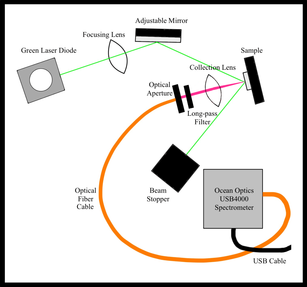
A schematic diagram of the experimental setup is shown in Fig. 1. The solid aluminum optical breadboard with 1/4-20 tapped holes was used as the baseplate for the experimental setup. A 5mW 530 nm green laser diode was used as the light source. A focusing lens (convex lens of 200 mm focal length) was used for focusing the laser beam onto a mirror. The mirror was used to direct the laser light onto the semiconductor sample. Semiconductor samples of GaAs, InP, In1-xGaxP, and CdTe nanoparticles were used for the experiment. The first three samples were mounted on a metal plate one above the other. The CdTe nanoparticles sample consisted of CdTe quantum dots on a microscope slide with a cover slip on top of it. The whole sample was further mounted on a metal plate. A collection lens (convex lens of 25 mm focal length) was used for focusing the photons emitted by the semiconductor sample into the optical aperture through the 590 nm long-pass optical filter. The filter absorbs photons of wavelength below 590 nm and allows photons of wavelength above 590 nm to pass through it. The filter also serves the purpose of filtering out any residual green light from the laser. The optical aperture was used to send the photons emitted by the sample into a 600 micron core optical fiber cable, which then sends the light into the spectrometer. The spectrometer used was the model USB2000-FLG by Ocean Optics. The spectrometer was connected to the computer using a USB cable. The OceanView software (from http://www.oceaninsight.com) was used for spectral analysis. Optical posts and post holders were used to fasten all the different components onto the breadboard.
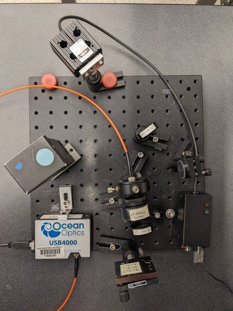
A picture of the actual experimental setup is shown in Fig. 2.
Results
PL spectroscopy of ambient light from fluorescent tube
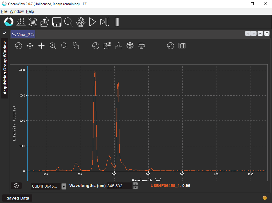
As shown in Fig. 3, there are six peaks in the PL spectrum. These peaks were found to occur at the following wavelengths in ascending order: 436.404 nm, 487.605 nm, 543.185 nm, 584.643 nm, 611.094 nm, and 708.436 nm. The narrowest line corresponds to peak 5 and its line-width (FWHM) was calculated to be 9.047 nm.
| Wavelength (nm) | Intensity (counts/second) | Element | |
| Peak 1 | 436.404 | 73138.286 | Hg |
| Peak 2 | 487.605 | 166630.857 | Tb3+ |
| Peak 3 | 543.185 | 909339.429 | Tb3+ |
| Peak 4 | 584.643 | 264228.571 | Tb3+/Eu3+:Y2O3 |
| Peak 5 | 611.094 | 828278.857 | Eu3+:Y2O3 |
| Peak 6 | 708.436 | 54253.714 | Eu3+:Y2O3 |
In the above table, Intensity in counts/second was found by dividing the peaks by the integration time, 4375 μs. The elements for the spectral peaks were found from the NIST database of spectra for mercury and an article on fluorescent light phosphors.
PL spectroscopy of the gallium arsenide sample
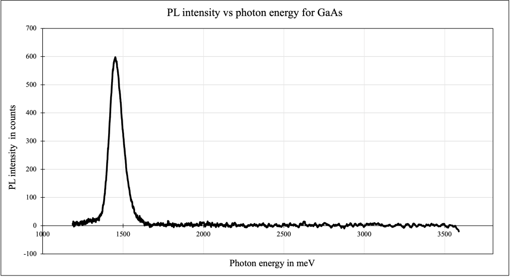
For the sample of GaAs, the peak was measured to occur at the wavelength 854.34 nm (photon energy of 1450.843 meV) and the line-width was calculated to be 55.434 nm (photon energy of 94.783 meV). The uncertainty in the peak photon energy is calculated to be 40.248 meV.
PL spectroscopy of the indium phosphide and unknown indium gallium phosphide samples
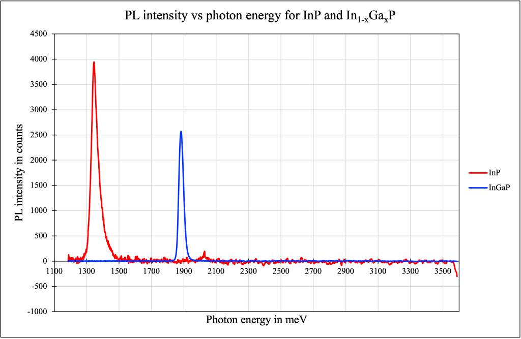
For the sample of InP, the peak was measured to occur at the wavelength 922.119 nm (photon energy of 1344.2 meV) and the line-width was calculated to be 32.648 nm (photon energy of 47.77 meV). The uncertainty in the peak photon energy is calculated to be 20.284 meV.
For the sample of In1-xGaxP, the peak was measured to occur at the wavelength 658.332 nm (photon energy of 1882.81 meV) and the line-width was calculated to be 32.648 nm (photon energy of 33.958 meV). The uncertainty in the peak photon energy is calculated to be 14.419 meV.
Using the formula E′(x) = E0 + 512 x + 603 x2, we write x as a function of E0 and E′, using x = {−512 ± √[5122 + (2412)(E′−E0)] / 1206} and calculate the gallium concentration. Here, E0 and E’ are the photon energy spectrum peaks of the InP (1344.2 meV) and In1-xGaxP (1882.81 meV) samples respectively.
This gives x = 0.6115, or in other words, the gallium and indium concentrations in the sample are 61.15% and 38.85%.
Thus, the band gap energies for samples of GaAs, InP, and In0.61Ga0.39P were experimentally observed to be 1.45 eV, 1.34 eV, and 1.88 eV.
PL spectroscopy of cadmium telluride nanoparticles
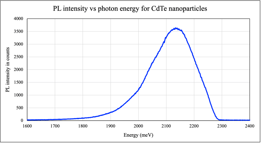
For the sample of CdTe quantum dots, the peak was measured to occur at the wavelength 581.058 nm (photon energy of 2133.20 meV) and the line-width was calculated to be 52.747 nm (photon energy of 191.97 meV). The uncertainty in the peak photon energy is calculated to be 81.518 meV.
The average diameter of the CdTe nanoparticles can be calculated using the Brus equation, E(x) = E0 + (ħ2π2/2md2). Rewriting the equation, we get d2 = ħ2π2/2m(E-E0). Here, E is 2133.2 meV, E0 is 1490 meV, and m is 0.09m0.
The diameter d is then calculated to be 2.5505 nm. The uncertainty in d was found to be 0.1616 nm using the ‘propagation of errors’ formula. Thus the average diameter of the CdTe nanoparticles is 2.5505 ± 0.1616 nm.
Discussion
PL spectroscopy of ambient light from fluorescent tube
The PL spectral analysis of the ambient light emanating from fluorescent tubes revealed that the spectral lines belong to mercury (Hg), terbium (Tb3+), and europium (Eu3+). The strongest spectral line belonged to terbium and europium. These results are as expected since modern fluorescent tubes use terbium-doped LaPO4 and europium-doped Y2O3 as phosphors. The spectral lines of mercury were detected since fluorescent tubes typically use a few milligrams of mercury which must be vaporized for the tube to work properly.
PL spectroscopy of the gallium arsenide sample
The value of the photon energy corresponding to the spectral peak of GaAs was calculated to be 1.451 eV. This is approximately equal to the well-known energy gap value of 1.424 eV for GaAs at 300 K. Furthermore, the spectral peak has a wavelength of 854.34 nm, which agrees with the fact that GaAs is used for infrared LEDs.
PL spectroscopy of the Indium Phosphide sample
The value of the photon energy corresponding to the spectral peak of InP was calculated to be 1.344 eV. This is equal to the well-known energy gap value of 1.344 eV for InP at 300 K. Furthermore, the spectral peak has a wavelength of 922.119 nm, which agrees with the fact that InP is used for infrared and microwave communication systems.
PL spectroscopy of the Indium gallium Phosphide alloy sample
The gallium concentration x was found to be 0.61 ± 0.02. The value of the photon energy corresponding to the spectral peak of In1-xGaxP was calculated to be 1.883 eV. This agrees with the fact that doping InP with Ga can increase its band gap energy. In fact, alloying materials with suitable other materials can increase band gap energy. Alloying is a very useful tool to manipulate band gap energies and change the color of the emitted light. The fact that the spectral peak changed to 658.332 nm, a wavelength in the visible range confirms this.
PL spectroscopy of cadmium telluride nanoparticles
When the size of particles become approximately less than 100 nm, the band gap energy of the nanoparticles shift to a higher value. This is a result of the quantum mechanical phenomenon called ‘quantum confinement’. This effect comes into play when the size of the particle is too small to be comparable to the wavelength of the electron and therefore the movement of the charge carriers are restricted due to the small volume. As a result, electrons or electron-hole pairs called “excitons” are tightly confined in all three dimensions. This confinement has consequences for the electrical, mechanical, and optical properties of the material. It is well-known fact that the band gap energy increases of CdTe increases as its size decreases.
In this experiment, the diameter of the CdTe nanoparticles was calculated to be 2.55 ± 0.16 nm, which is much smaller than 100 nm and therefore quantum confinement causes a shift in the band gap energy.
Conclusion
In this experiment, PL spectroscopy was done to analyze the band gap energies of semiconductor samples of GaAs, InP, a sample of InP doped with Ga, and a sample of CdTe nanoparticles. Furthermore, the effect of doping and quantum confinement on band gap energies were studied.
Click here to access my lab report for this project.

One thought on “Photoluminescence Spectroscopy of Semiconductors”